
Home>Research
Prof. Ray's research group has been carrying out several multidisciplinary Applied Physics and Materials Science-based problems, focusing on the fabrication of photonic, electronic, optoelectronic, photovoltaic, sensor, and memory devices using various semiconducting nanostructures, epitaxial thin films and their hybrids ranging from Group-IV materials (Si, Ge, Sn) to II-VI semiconductors (ZnO, CdS, ZnS etc.), plasmonic metal nanostructures (Au, Ag) to 2D materials (graphene, graphene oxide, MoS2, WS2, black phosphorous etc.). Recently, Prof. Ray has also started working on amalgamating perovskites with other traditional semiconductors for fabricating optoelectronic devices. In addition, some hybrid bio-photonic and memory devices have also been fabricated by integrating silk proteins and Au nanoparticles in a collaborative work which opened a new path towards bio-integrable device applications. For the fabrication of nanostructures, our research group relies on both physical and chemical routes. Various sophisticated physical deposition techniques such as Molecular Beam Epitaxy (MBE), RF sputtering, Pulsed Laser Deposition (PLD), Chemical Vapour Deposition (CVD), Vapour Liquid Solid (VLS) have been established as in-house facilities in the “Microscience Lab”. For the chemical synthesis of semiconductors, plasmonic nanostructures and 2D materials, we have developed a chemical synthesis lab with required facilities. Easy access to Electron Beam Lithography facility of the institute is available for nanofabrication of devices. Essential characterization tools include Atomic Force Microscopy (AFM), X-Ray Diffractometer (XRD), Steady-state and time-resolved measurement facilities are available in the lab. The lab is well equipped to perform various optical, electrical and optoelectronic measurements on the fabricated devices and study their performances. With some of our collaborators, we integrate our wide variety of material nanostructures for non-linear photonics, THz absorption, gas sensing, soft lithography patterning etc.
Thanks for funding us


Group IV (Si, Ge, Sn) thin films & heterostructures for optoelectronic and memory devices
This is the research area on which we are working on for a decade and the results are considered as significant breakthroughs for future nanodevice applications. In this context, we are mainly interested in developing pseudomorphic strained Si-Ge alloy heterostructures for high mobility MOSFETs to low dimensional quantum structures. Fabrication of Ge quantum dots, Ge-Sn alloy and


2D materials and their applications for optoelectronic devices
This is the newest research area we are involved with most diverse range of materials and opportunities. Starting with graphene and graphene oxide, over the recent years, we started synthesizing MoS2, WS2 flakes and quantum dots for their utilization in photodetectors and LEDs. Black phosphorous, MoSe2, PbS nanocrystals, graphene quantum dots are some of the current materials we are highly focused on. We explore their optoelectronic properties depending on nanocrystal size and nature of surface modifications.

II-VI semiconductors and their applications for optoelectronic, memory and gas sensing devices
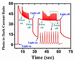
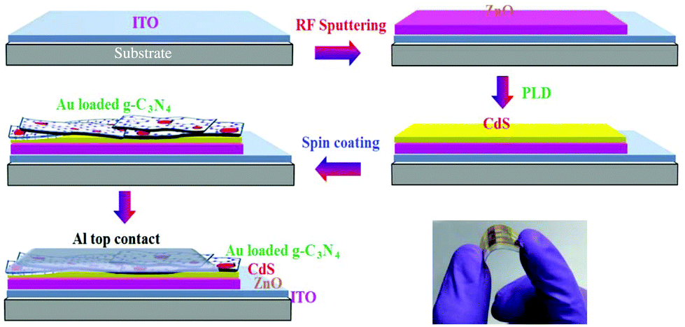
Wide bandgap II-VI semiconductors (ZnO, CdS, ZnS) with their unique optical properties in the visible spectrum offer great potential for optoelectronic and photovoltaic devices. We work on developing high performances solar cells, photodetectors, photo-transistors using ZnO, CdS nanostructures and their heterostructures. We also study the plasmonic effect in the optical properties of these


Inorganic perovskites for optoelectronic devices
We are involved in advanced research in perovskites (ABX3). We specially focus on synthesis of comparatively stable perovskites in high yield for large area photonic applications. All inorganic perovskites (CsPbX3: X = Cl, Br, and I) are very promising for the development of next-generation optoelectronic and photovoltaic (PV) devices. Inorganic perovskites are important due to its high diffusion length, high absorption coefficient, excellent charge transport properties, and high photostability. in these perovskites, cation or anion substitution can change the optical absorption edge, with or